20+ d flip flop block diagram
The working of the clap switch is discussed through the block diagram of the clap switch. In the above block diagram an audio power amplifier is used to amplify audio signals with less power to a level appropriate for controlling loudspeakers.
Flip Flop Circuit Types And Its Applications
It contains 20 pins which have three-state output.

. 6 to 30 characters long. From the figure you can see that the D input is connected to the S input and the complement of the D input is connected to the R input. In D flip flop the output after performing the XOR operation of the T input with the output QPREV is passed as the D input.
These devices can be used for shift register applications and by connecting Q output to the data input for counter and toggle applications. D flip-flop also known as Data flip-flop shifts one bit from the input side to the output side if and only when the clock changes the transition from a high state to a low state or low state to a high state. Our global writing staff includes experienced ENL ESL academic writers in a variety of disciplines.
The result is that the flip-flop looses control of Q and Q and if the two inputs are now switched HIGH again after this condition to logic 1 the flip-flop becomes unstable and switches to an unknown data state based upon the unbalance as shown in the following switching diagram. In the circuit diagram of the decade counter the operation is explained in four stages where every stage is included with a flip flop. The logic level present at the D input is transferred to.
Find a wide range of affordable and stylish furniture online. The Institute comprises 33 Full and 13 Associate Members with 12 Affiliate Members from departments within the University of Cape Town and 12 Adjunct Members based nationally or internationally. In the block diagramQ of RS Flip flop is connected no whereI think it must be connected to the the discharge transistorPlease get it corrected.
Likewise if you want to transfer four bits of data you need 4 flip-flops. In the two-phase synchronous systems to avoid the transit count the data latches D-Latches are used. L 880 x W 9401670 x H 5101030 mm.
A voltage or current applied to one pair of the transistors terminals controls the current. Level the flip-flop is set and the output goes high. In computer engineering a hardware description language HDL is a specialized computer language used to describe the structure and behavior of electronic circuits and most commonly digital logic circuits.
The Block diagram of the T flip-flop is given below where T defines the Toggle input and CLK defines the clock signal input. Dark Brown or Iceberg. When RESET goes low the flipflop is -.
These will be the first sequential circuits that we code in this course on VHDL. Here D represents input data. T Flip Flop Circuit.
The logical circuit of the T flip flop by using the D flip flop. A dynamical system may be defined formally as a measure-preserving transformation of a measure space the triplet T X Σ μ ΦHere T is a monoid usually the non-negative integers X is a set and X Σ μ is a probability space meaning that Σ is a sigma-algebra on X and μ is a finite measure on X ΣA map Φ. ASCII characters only characters found on a standard US keyboard.
The circuit diagram and truth table is given below. It is composed of semiconductor material usually with at least three terminals for connection to an electronic circuit. Seat with Pocket Spring Webbing.
Basic D Flip-Flop. All the flip-flops are mainly controllable by the clock and enable pin. One of the official and widely used PLC programming languages is the Function Block Diagram FBD.
Half Leather - 0911mm. As one of the inputs on the AND function is Q1 which also acts the output for the whole block. In electronics a flip-flop or latch is a circuit that has two stable states and can be used to store state information a bistable multivibratorThe circuit can be made to change state by signals applied to one or more control inputs and will have one or two outputs.
D flip flop is actually a slight modification of the above explained clocked SR flip-flop. S-R Flip-flop Switching Diagram. CLK indicates clock pulses.
The reset RESET input can override all other inputs and can be used to initiate a new timing cycle. A transistor is a semiconductor device used to amplify or switch electrical signals and powerThe transistor is one of the basic building blocks of modern electronics. We will code all the flip-flops D SR JK and T using the behavioral modeling method of VHDL.
What is the Difference Between Latches and Flip-Flops. This block diagram includes an audio amplifier bistable flip flop circuit amplifier. It is the basic storage element in sequential logicFlip-flops and latches are fundamental building blocks of digital.
The block diagram of 3-bit Asynchronous binary down counter is similar to the block diagram of 3-bit Asynchronous binary up counter. A complete tutorial of 555 Timer IC with its block diagram working of SENE 555 TimerPin Configuration and pin out diagram Download 555 data sheet. This lets us find the most appropriate writer for any type of assignment.
Many call this a flip-flop function. But the only difference is that instead of connecting the normal outputs of one stage flip-flop as clock signal for next stage flip-flop connect the complemented outputs of one stage flip-flop as clock signal. The negative edge D flip-flop can be represented with a triangle and a bubble at the clock end of the D flip-flop block diagram.
So the circuits hold the capability of counting 16 states means 16 bits where only 10 out of 16 are utilized. Each flip Flop has different input. 20 LED related 3 Light Related 14.
Lets write the VHDL code for flip-flops using behavioral architecture. The usage of pulse latches follows the same behavior of flip-flops but good enough to generate a quick response. Q1 will remember that at.
If the trigger input is above the trigger level and the threshold input is above the threshold level the flip-flop is reset and the output is low. Furniture Mart is the largest online furniture store in Singapore specialising in latest designer furniture Mattresses Bed Frames Wardrobes Sofa Sets for Living room Bed room Dining room and Offices. A hardware description language enables a precise formal description of an electronic circuit that allows for the automated analysis and simulation of an electronic circuit.
Well also write the testbenches and generate the final RTL schematics and simulation waveforms for each flip-flop. Must contain at least 4 different symbols. Negative Edge Triggered D flip flop Circuit Diagram.
It is widely used to store the data and the codes for computations. X X is said to be Σ-measurable if and only if for every σ. Each flip-flop has independent data set reset and clock inputs and Q and Q outputs.
It is a simple and graphical way to program any functions together in a PLC program.

Hedging Strategy For An American Put Option With Strike 20 And S 0 20 Download Scientific Diagram

Qca Layout Of Two Input Xor Gate 20 Download Scientific Diagram

Block Diagram Of The Receive Path For The Ettus Research Wbx Rf Download Scientific Diagram
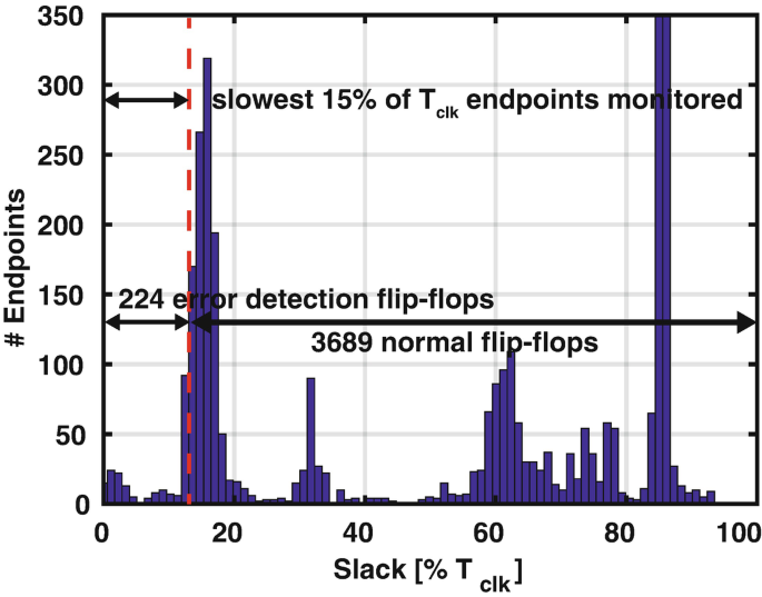
Timing Error Aware Microcontroller Springerlink

A Schematic Of Each D Flip Flop Used In The Design B Schematic Of The Download Scientific Diagram
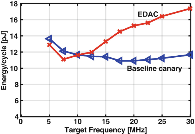
Timing Error Aware Microcontroller Springerlink

Diy Aluminum Pop Tab Handbag Pop Tabs Pop Tab Purse Pop Tab Crafts
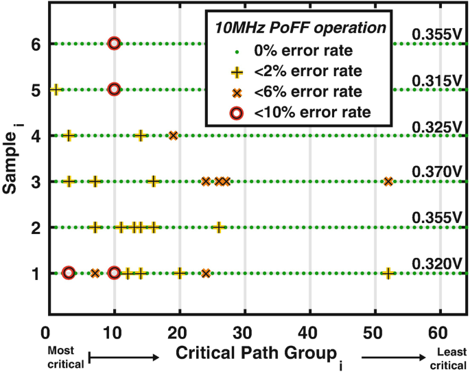
Timing Error Aware Microcontroller Springerlink
A Digital Quartz Clock From Scratch By Erik Van Zijst Medium

A Proposed Synapse Block Architecture B Arbiter Fsm Showing The Download Scientific Diagram

Ampa Receptor Sequences For R G Editing And Flip Flop Alternative Download Scientific Diagram
![]()
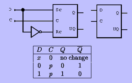
Schematic Diagram Of A Conventional D Flip Flop Download Scientific Diagram
![]()
A Pulse Sequence For Nmr Spectroscopy And Nuclear Rabi Oscillations Download Scientific Diagram

Cholesterol Distribution In Small Unilamellar Vesicles The Journal Of Physical Chemistry B

Top Level Block Diagram Of The 4 1 Data Multiplexer Download Scientific Diagram
1 Basic Signal Processing System 13 Download Scientific Diagram

A Phase Detector Block Diagram B Dynamic Flip Flop Circuit Download Scientific Diagram